=
The pre-amplifier schematic is shown in Figure 4.
We have prototyped this design and thoroughly characterized it's AC and
DC performance.
The design is an unfolded cascode which is similar to our previous
prototype. We have doubled the input transistor width and adjusted some
passive component values, which reduced the input impedance ![]() to
to
![]() and increased the gain to about 1.4mV/fC. The peaking time
for a
and increased the gain to about 1.4mV/fC. The peaking time
for a ![]() input charge is 5nS.
input charge is 5nS.
A summary of the specified, simulated and measured performance is shown in Table 3.1. The input impedance, peaking time and noise performance are all close to specification, and this prototype clearly shows that the desired performance can be achieved in CMOS.
The noise performance was estimated using Equation 1, and measured on
the prototype chip. The results are compared in Figure 5.
Note that this is a two-pole approximation, which is not strictly
correct for large values of ![]() , however this expression is a close
approximation for small values (the terminated MDT is 360
, however this expression is a close
approximation for small values (the terminated MDT is 360 ![]() ). Two
sets of measured noise points are shown, for two amplifier bias current
settings. 1mA is the nominal operating current, while the 2mA setting
shows somewhat improved noise performance.
). Two
sets of measured noise points are shown, for two amplifier bias current
settings. 1mA is the nominal operating current, while the 2mA setting
shows somewhat improved noise performance.
The other parameters used in the calculation were a peaking time ( ![]() )
of 15nS and an input capacitance (
)
of 15nS and an input capacitance ( ![]() ) of 6pF (3pF from the amplifier
and 3pF from stray capacitance).
) of 6pF (3pF from the amplifier
and 3pF from stray capacitance).
The 360 ![]() terminator contributes
about 4000 electrons, and the amplifier increases the total noise to
about 6000 electrons, or about 1fC. Our expected threshold signal for
20 primary electrons in the MDT is 50fC, giving us an SNR of at least 50:1.
A complete noise analysis has been presented elsewhere[4].
terminator contributes
about 4000 electrons, and the amplifier increases the total noise to
about 6000 electrons, or about 1fC. Our expected threshold signal for
20 primary electrons in the MDT is 50fC, giving us an SNR of at least 50:1.
A complete noise analysis has been presented elsewhere[4].
![]()
=
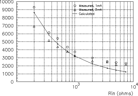
Figure 5: Equivalent Noise Charge (e) vs Input Resistance. 1mA is the
nominal operating current, while 2mA gives somewhat improved noise
performance.

